A Comprehensive Guide to PCB Design Review
When it comes to PCB (Printed Circuit Board) design, a meticulous review process is crucial to ensure functionality, manufacturability, and cost-effectiveness. Let’s dive into the essential checklist items you should consider before sending your design off for production.
Silkscreen Clarity and Placement
Ensure all silkscreen labels are clear and correctly placed. Misaligned labels, especially those over bare copper or holes, can lead to confusion during assembly and potential errors in component placement and soldering.
PCB Size and Shape
The size and shape of your PCB can significantly impact manufacturing costs and technical feasibility. Both extremely large and small boards can pose challenges. Irregular shapes might also complicate the manufacturing process. Always consider these factors to optimize for both cost and manufacturability.
Mechanical Mounting Holes
Verify the location and size of all mechanical mounting holes. Ensure there’s enough clearance around each hole for screw heads and standoff spacers, on both sides of the PCB. Moving these holes after design completion can be very challenging, so get it right the first time. Remember that some components may also require their own mounting holes, such as connectors with mechanical fasteners or guide pins.
Component Placement
Component placement is critical, especially for parts like connectors, buttons, switches, and LEDs. Misplaced components can interfere with the final assembly, affecting how the PCB fits into its enclosure or connects to other parts.
Silkscreen Component Orientation Marks
Every directional component should have clear orientation marks on the silkscreen. Incorrectly oriented components can lead to malfunction, so these markings assist in correct placement and troubleshooting.
Fiducial Marks
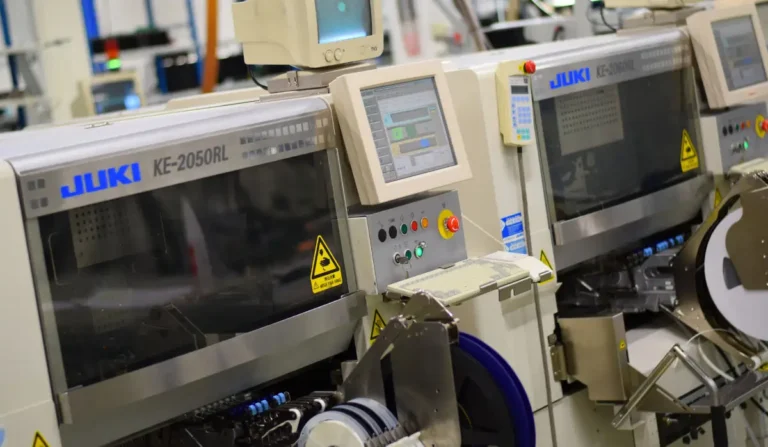
Automatic component placement machines require at least three fiducial marks, spaced well apart. These marks should be on both sides of the PCB if components are mounted on both sides. Fiducial marks are crucial for all automated steps in the production process, making their absence a common but significant oversight.
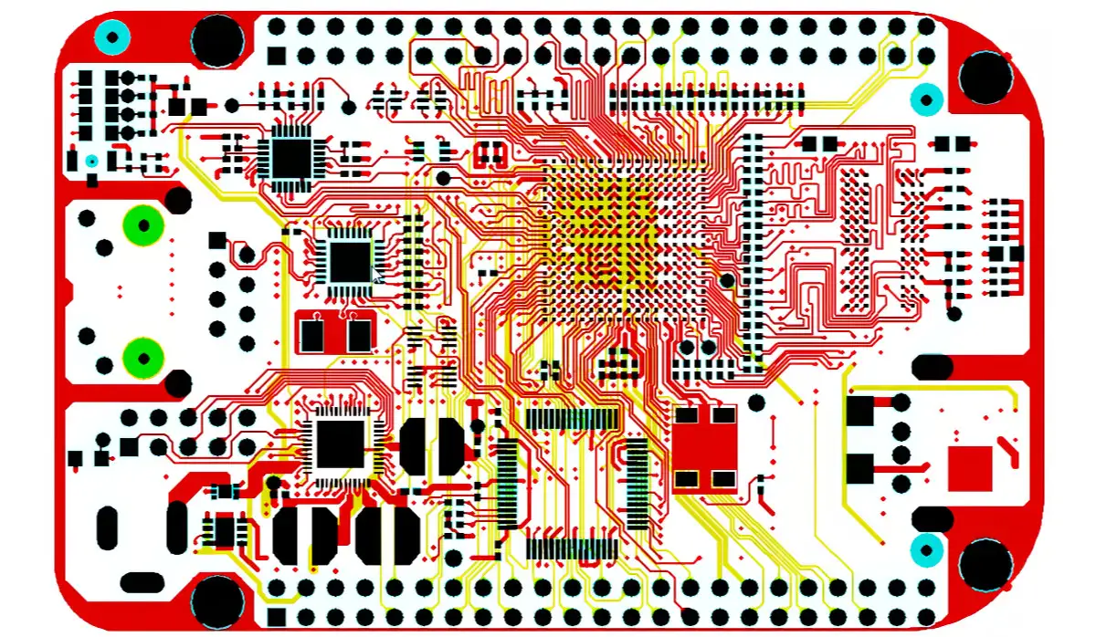
Component Footprints
Ensure the footprints on the PCB match the components listed in the bill of materials (BOM). Mismatched footprints can cause significant issues during assembly.
Placement Drawing
Check the placement drawing for clear orientation marks and ensure all components and their positions are accurately represented. Text in the placement drawing should be legible and not mirrored.
Bill of Materials (BOM)
The BOM should include all necessary information:
- Quantity (QTY)
- Position on PCB (REFERENCE DESIGNATOR)
- Component name (PART)
- Full description (PART DESCRIPTION)
- Manufacturer (MANUFACTURER)
- Manufacturer’s code (MANUFACTURER CODE)
- Package type (PACKAGE TYPE)
- Mounting method (SMD/THRU-HOLE)
Gerber Files
Gerber files are essential for manufacturing the PCB and stencils. Make sure all necessary layers are included: copper layers, drill files, solder mask, stencil layers, etc.
SMD Component Placement Coordinates (XY Data)
Automated placement machines and automated optical inspection machines (AOI) use XY coordinate files to position SMD components. Ensure the file includes:
- Component positions
- X and Y coordinates
- Alignment marks’ coordinates
- Component orientations/angles
- The side of the PCB for component placement
For consistency, the origin point (0,0) should ideally be in the lower left corner of the PCB, and this should be clearly stated in the XY data file.
By following this comprehensive checklist, you can streamline your PCB design process, minimize errors, and ensure a smoother manufacturing experience. Happy designing!